01 / Wavelength1
850 nm or 940 nm selection
Review sensor sensitivity, ambient-light behavior and eye-safety assumptions before choosing the emitter family.
850 nm / 940 nm
3D SENSING SOLUTION
A reference-style solution page for teams evaluating VCSEL emitters, arrays and compact modules for depth perception systems.
Use this page to align wavelength, optical power, beam shape, package size and thermal limits before selecting samples or starting a custom module conversation.

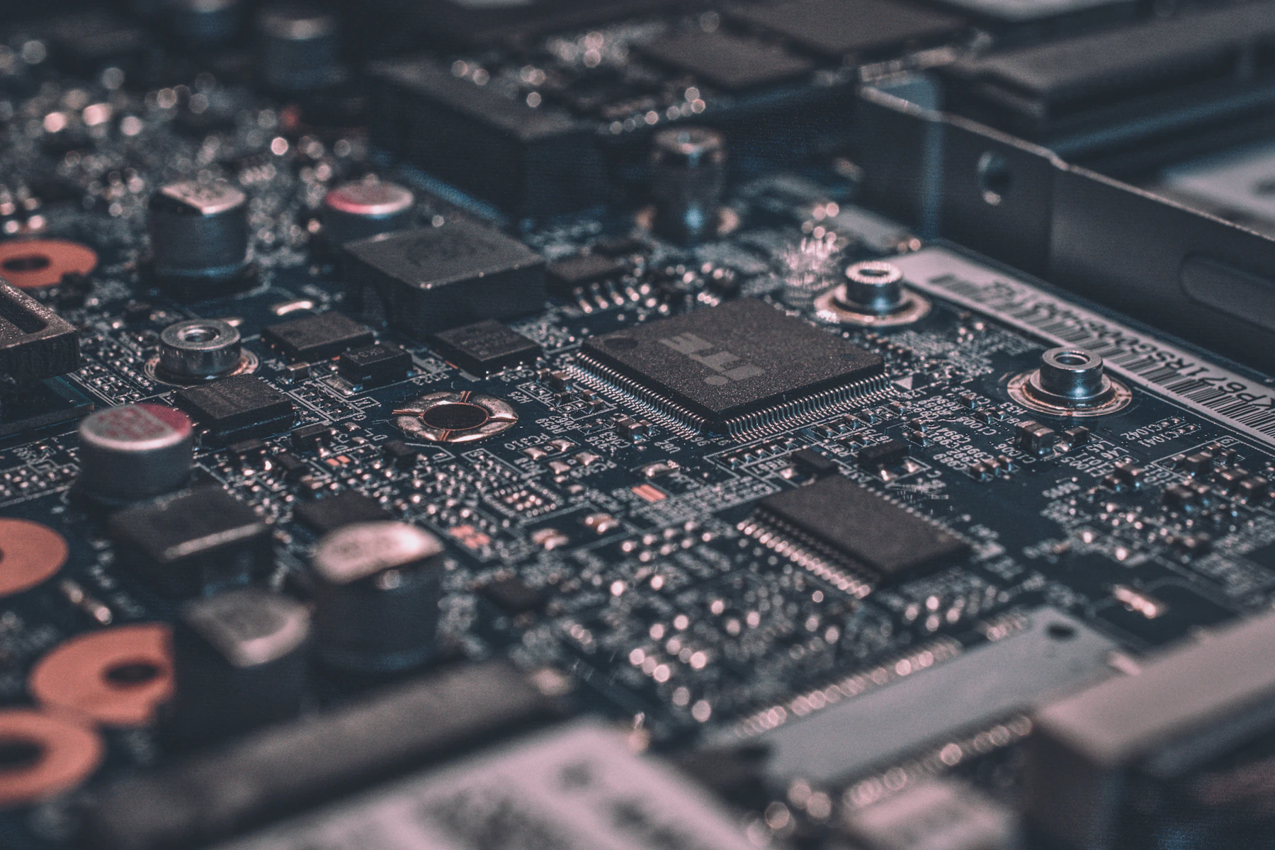
APPLICATION OVERVIEW
VCSEL selection starts with the imaging method: ToF, structured light, proximity sensing or gesture recognition.
The emitter package, beam pattern and driver interface need to be reviewed together because the optical target is tied to camera FOV, duty cycle, ambient light and available thermal area.
SAME SOLUTION-PAGE MODULE PATTERN
The module structure mirrors the reference solution template: proof rows, media sections, product recommendation and CTA.
Review sensor sensitivity, ambient-light behavior and eye-safety assumptions before choosing the emitter family.
Match divergence, diffuser or DOE needs with the camera field of view and working distance.
Coordinate peak current, pulse width, board copper, package choice and test duty cycle.
Compare multiple emitters in the same fixture before committing to a custom mechanical outline.

ENGINEERING SUPPORT
The right emitter still needs usable drive conditions, a stable optical stack and measurable test criteria.
PhotonEdge demo pages use standard modules to show how an engineer can move from solution context into product comparison, then into sample or ODM requests.
RECOMMENDED FOR 3D SENSING
Bare die, ToF packages and compact modules that fit common depth-sensing prototype paths.
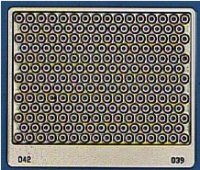
High-uniformity 940 nm VCSEL die for ToF depth cameras, structured-light engines, face authentication, and proximity modules.
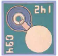
850 nm VCSEL bare die for short-reach optical data links, sensing references, and compact optical transmitter builds. 850 nm VCSEL bare die for short-reach optical data links, sensing references, and compact optical transmitter builds.
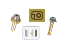
Compact packaged 940 nm VCSEL emitter with controlled divergence for ToF depth sensing and proximity measurement. Compact packaged 940 nm VCSEL emitter with controlled divergence for ToF depth sensing and proximity measurement.
High-power VCSEL array platform for LiDAR, industrial depth sensing, gesture capture, and long-range NIR illumination. High-power VCSEL array platform for LiDAR, industrial depth sensing, gesture capture, and long-range NIR illumination.
RELATED ENGINEERING NOTES
Use the notes section to review selection cases and module-request preparation.

A demo case note on choosing wavelength, beam profile, package, and driver assumptions for a compact ToF depth module.

A short application case for driver monitoring and occupant sensing teams comparing VCSEL NIR illumination choices.

A practical checklist for wavelength, optical power, beam shape, drive mode, thermal path, compliance, and pilot-run planning.
START A 3D SENSING PROJECT
Send the wavelength, field of view, working distance and package constraints. The request will be routed into the ODM workflow.
Standard samples and custom assemblies can be reviewed together.
Depth-sensing VCSEL sample and module planning
ToF / structured light / proximity